
X-rays let you see the smallest feature buried in your CPU

Tags: Your CPU

X-rays let you see the smallest feature buried in your CPU published by nherting
Writer Rating: 0
Posted on 2017-03-30
Writer Description: current events
This writer has written 195 articles.
The semiconductor industry is beyond remarkable when it comes to the complexity and precision of processes. A modern integrated circuit is not a single layer of circuitry, but many layers, all stacked on top of each other. This is all done through photolithography, where a pattern is imaged on a silicon wafer. Each layer requires a separate image, and all the images have to be aligned. If you take the 14nm number seriously (a nanometer is 1/1,000,000th of a millimeter), then wafers and masks, which are seriously hold-in-two-hands-big, have to be aligned with a precision that is better than the feature size. But, how do you know you've done it right?
The obvious answer is whether or not the chip works. But it would be nice to image the circuit so that it can be compared to the design. Apart from detecting problems during manufacturing, being able to image the final product would also allow for the design to be improved, since it would let you identify areas of a chip that consistently cause problems. But, how do you image structures that might be as small as 14nm that are buried under other structures that you also want to image?
The answer, it seems, is a form of X-ray tomography.
3D images from buried structures
We're all pretty familiar with the idea of getting an X-ray, which is a form of shadow imaging. The bones absorb more X-ray radiation than the surrounding flesh, creating a shadow. The X-ray image shows the contrast between bone and flesh, allowing doctors to pinpoint fractures and, ahem, buried objects.
You may be less familiar with X-ray crystallography. In crystallography, the X-rays are scattered by the atoms in a crystal. Because the atoms are arranged in a regular pattern, the 2D pattern of the scattered X-rays reveals the 3D structure of the crystal. This only works because the 3D pattern repeats itself many, many times, allowing the scattering of individual atoms to be amplified.
An integrated circuit is somewhere in between these two. The circuit consists of materials with different densities: some scatter X-rays strongly, others weakly. Some are crystalline, some are not. However, the X-rays penetrate deeply enough that the scattered radiation contains all the information about the entire structure. In principle, a single snapshot of the scattering pattern should allow the 3D image to be reconstructed.
But, it doesn't. The reason is that we record the X-ray intensity and not the amplitude. The difference between the two is the phase of the radiation. The bright spots in the scattering pattern record locations for which the phases of different X-rays add up constructively, but the constructive interference can be achieved in any number of ways. Absent the regular structure of a crystal, there's no way of telling which one of these ways produced what you're seeing. In other words, an infinite number of 3D structures can supply the same intensity distribution.
Making the infinite finite
The way around the problem is to eliminate the numerous incorrect structures by insisting that the integrated circuit has a single, consistent structure. Take a single X-ray scattering pattern from a section of chip. Then rotate the chip and take another pattern. The structure that generated the pattern is the same in both cases, even though the patterns are different. You can keep doing this for different angles and different but overlapping areas of the integrated circuit.
You end up with many, many different X-ray scattering patterns that all correspond to the same underlying structure. This constrains the phases of the scattering X-rays. You feed the data to a sort of mathematical guess and correct-the-guess routine, which iterates until it determines the one unique structure that generated all the scattering patterns.
This is a common technique in many 3D imaging schemes. But, in X-ray imaging it was kind of rare because the sources are so pathetically weak. Essentially, it takes a very long time to obtain each pattern, and you need a lot of patterns. By the time you've finished imaging, management has brought you your golden watch.
I knew my free electron laser would come in handy
Avoiding this time sink is the key to the results published by the Paul Scherrer Institute. The researchers at the institute have access to a nice bright source of X-rays, so they can do this sort of imaging, albeit still too slowly to be interesting for industrial applications.
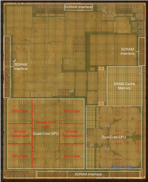
The paper has two key points to it. First, they show that it works. They obtain very good images from an older generation ASIC and from an Intel Pentium G3260, which has some features as small as 22nm. In both cases, the researchers obtained high-quality 3D images—even showing the edge roughness on the interconnect wires. That is pretty cool and is a clear demonstration that the technology works well.
The second point to the paper was to note that there are a whole lot of new free electron lasers coming on line. Their imaging technique, combined with some optimization in the detector, turned over to these new, very bright X-Ray sources, mean that images of even very complex chips could be obtained quickly.
Now, of course, not even Intel has a free electron laser in the fab. But all of the facilities with this sort of hardware sell companies access to it. Especially early in the development cycle, it may be well worth buying time if it cuts down on the problems with bringing a new chip to market.
Sources:
https://arstechnica.com/science/2017/03/bright-x-rays-reveal-3d-structure-of-processors-and-defects-lurking-within/
You have the right to stay anonymous in your comments, share at your own discretion.